- 您现在的位置:买卖IC网 > Sheet目录409 > DR8001-DK (RFM)3G DEVELOPMENT KIT 868.35MHZ
�� �
�
�868.35� MHz�
�Transceiver� Module�
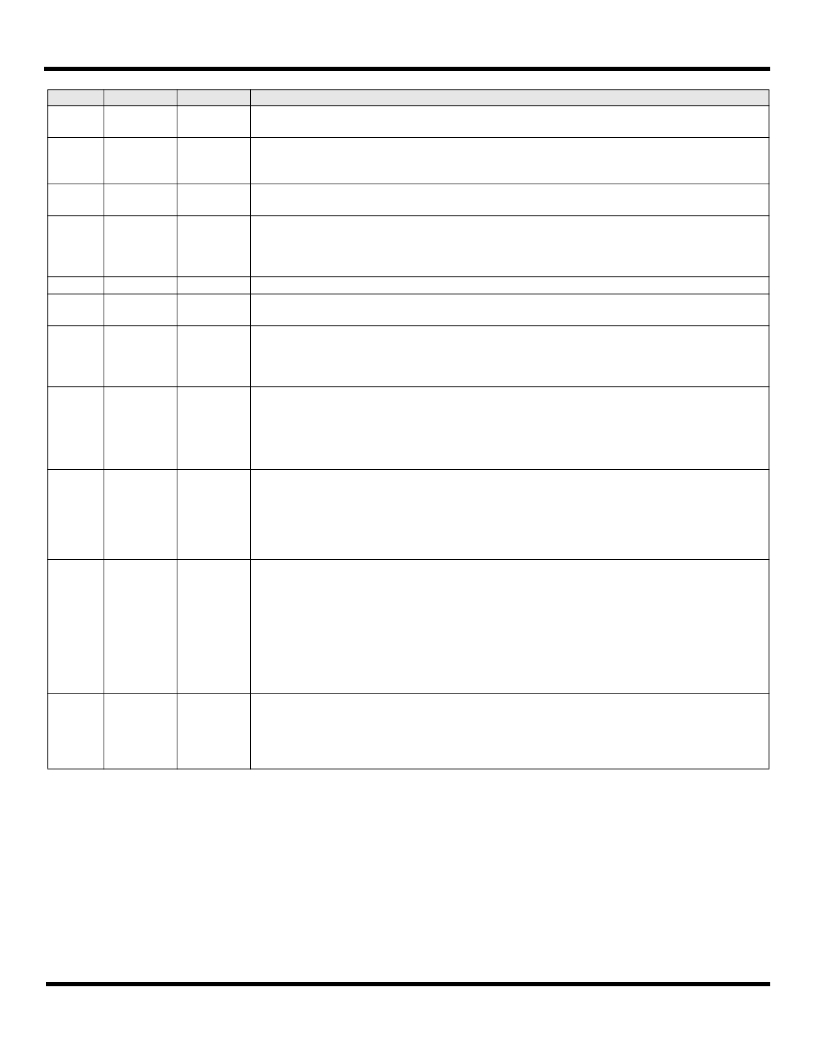
�Pin�
�8�
�Name�
�TX/RX�
�In/Out�
�In�
�Description�
�Logic� Input� (CMOS� compatible).� This� pin,� in� 3G� mode,� selects� the� operation� of� the� TR8001� .� Pull� this� pin�
�‘High’� for� Transmit� Mode.� Pull� this� pin� ‘Low’� for� Receive� mode.� Do� not� allow� this� pin� to� float.�
�Logic� Input� (CMOS� compatible).� This� pin,� in� 3G� mode,� selects� the� operation� of� the� TR8001.� Pull� this� pin�
�9�
�OOK/ASK�
�In�
�‘High’� for� OOK� Transmit/Receive� mode.� Pull� this� pin� ‘Low’� for� ASK� Transmit/Receive� mode.� Do� not� allow� this�
�pin� to� float.�
�10�
�SLEEP�
�In�
�Logic� Input� (CMOS� compatible).� This� pin,� in� 3G� mode,� puts� the� TR8001� into� Sleep� mode.� Pull� this� pin� ‘High’�
�for� Sleep� Mode.� Pull� this� pin� ‘Low’� for� operation� mode.� Do� not� allow� this� pin� to� float.�
�Logic� Input� (CMOS� compatible).� This� pin,� in� 3G� mode,� enables� the� Start� Vector� Recognition� circuit.� The�
�11�
�SVEN�
�In�
�TR8001� will� not� output� a� recovered� clock� on� RXDCLK� (pin� 16)� until� the� start� vector,� 0xE2E2,� has� been� recog-�
�nized.� Pull� this� pin� ‘High’� to� enable� Start� Vector� Recognition.� Pull� this� pin� ‘Low’� then� ‘High’� to� reset� the� Start�
�Vector� Recognition� circuit.� Do� not� allow� this� pin� to� float.�
�12�
�13�
�Not� Used�
�Not� Used�
�Keep� this� pin� pulled� ‘Low’.�
�Keep� this� pin� pulled� ‘Low’.�
�Logic� Input� (CMOS� compatible).� This� pin,� in� 3G� mode,� selects� the� receive� data� rate� of� the� DR8001.� Pull� this�
�14�
�4.8KBPS/�
�19.2KBPS�
�In�
�pin� ‘High’� to� select� 4.8kbps.� Pull� this� pin� ‘Low’� to� select� 19.2kbps.� Do� not� allow� this� pin� to� float.�
�NOTE:� Operating� at� 19.2kbps� will� require� the� value� of� C4,� C5� and� R4� to� change� to� accommodate� the�
�higher� data� rate.� See� the� TR8001� datasheet� for� recommended� component� values.�
�Logic� Input� (CMOS� compatible).� This� pin� sets� the� processor� to� operate� in� 3G� mode.� The� power-up� operating�
�configuration� of� the� TR8001� device� is� controlled� by� the� J2� jumper� setting.� When� DC� power� is� applied� to� the�
�15�
�3G� SEL�
�In�
�DR8001� with� J2� installed� across� 2-3,� this� pin� should� be� pulled� ‘High’� immediately� after� power-up� to� initiate� 3G�
�mode.� Failure� to� pull� pin� 15� ‘High’� after� power-up� will� cause� the� processor� to� remain� inactive.� Pulling� this� pin�
�‘High’� wakes� the� processor� for� 3G� mode� operation.� When� DC� power� is� applied� to� the� DR8001� with� J2� installed�
�across� 1-2,� this� pin� should� be� held� ‘Low’� to� operate� in� 2G� mode.� Do� not� allow� this� pin� to� float.�
�RXDCLK� is� the� clock� output� from� the� data� and� clock� recovery� circuit.� RXDCLK� is� a� CMOS� output.� When� the�
�radio’s� internal� data� and� clock� recovery� circuit� is� not� used,� RXDCLK� is� a� steady� low� value.� When� the� internal�
�16�
�RXDCLK�
�Out�
�data� and� clock� recovery� is� used,� RXDCLK� is� low� until� a� packet� start� symbol� is� detected� at� the� output� of� the�
�data� slicer.� Each� bit� following� the� start� symbol� is� output� at� RXDATA� on� the� rising� edge� of� a� RXDCLK� pulse,�
�and� is� stable� for� reading� on� the� falling� edge� of� the� RXDCLK� pulse.� Once� RXDCLK� is� activated� by� the� detec-�
�tion� of� a� start� symbol,� it� remains� active� until� SVEN� (pin� 11)� is� reset.� See� Pin� 11� description.�
�In� 3G� control� mode,� CFGDAT� is� a� bi-directional� CMOS� logic� pin.� When� CFG� (Pin� 19)� is� set� to� a� logic� 1,� con-�
�figuration� data� can� be� clocked� into� or� out� of� the� radio’s� configuration� registers� through� CFGDAT� using� CFG-�
�CLK� (Pin� 18).� Data� clocked� into� CFGDAT� is� transferred� to� a� control� register� each� time� a� group� of� 8� bits� is�
�received.� Pulses� on� CFGCLK� are� used� to� clock� configuration� data� into� and� out� of� the� radio� through� CFGDAT.�
�17�
�CFGDAT�
�In/Out�
�When� writing� through� CFGDAT,� a� data� bit� is� clocked� into� the� radio� on� the� rising� edge� of� a� CFGCLK� pulse.�
�When� reading� through� CFGDAT,� data� is� output� on� the� rising� edge� of� the� CFGCLK� pulse� and� is� stable� for� read-�
�ing� on� the� falling� edge� of� the� CFGCLK.� Refer� to� the� TR8001� datasheet� for� detailed� timing.� This� pin� is� a� high�
�impedance� input� (CMOS� compatible)� in� 2G� mode.� This� pin� must� be� held� at� a� logic� level.� Do� not� allow� this� pin�
�to� float.�
�In� 3G� control� mode,� pulses� on� CFGCLK� are� used� to� clock� configuration� data� into� and� out� of� the� radio� through�
�CFGDAT� (Pin� 17).� When� writing� to� CFGDAT,� a� data� bit� is� clocked� into� the� radio� on� the� rising� edge� of� a� CFG-�
�18�
�CFGCLK�
�In/Out�
�CLK� pulse.� When� reading� through� CFGDAT,� data� is� stable� for� reading� on� the� falling� edge� of� the� CFGCLK.�
�Refer� to� the� TR8001� datasheet� for� detailed� timing.� This� pin� is� a� high� impedance� input� (CMOS� compatible)� in�
�2G� mode.� Do� not� allow� this� pin� to� float.�
�RF� Monolithics,� Inc.� Phone:� (972)� 233-2903� Fax:� (972)� 387-8148�
�RFM� Europe� Phone:� 44� 1963� 251383� Fax:� 44� 1963� 251510�
�?1999� by� RF� Monolithics,� Inc.� The� stylized� RFM� logo� are� registered� trademarks� of� RF� Monolithics,� Inc.�
�E-mail:� info@rfm.com�
�http://www.rfm.com�
�DR8001-071107�
�Page� 4� of� 8�
�发布紧急采购,3分钟左右您将得到回复。
相关PDF资料
DR8100-DK
3G DEVELOPMENT KIT 916MHZ
DS1720S/T&R
IC THERMOMETER/STAT DIG 8-SOIC
DS1820
IC DGTL THERMOMETER TO92-3
DS1822+PAR
IC THERMOMETER ECONO DIG TO-92
DS1822Z/T&R
IC THERMOMETER ECONO DIG 8-SOIC
DS1870E-010+T&R
IC CNTRLR RF POWER AMP 16TSSOP
DS18S20-PAR+T&R
IC THERM MICROLAN HI-PREC TO-92
DS60R+T&R
IC SENSOR MICRO CENTIGRADE SOT23
相关代理商/技术参数
DR8001-EV
功能描述:射频开发工具 3G Transceiver Eval Module 868.35 MHz RoHS:否 制造商:Taiyo Yuden 产品:Wireless Modules 类型:Wireless Audio 工具用于评估:WYSAAVDX7 频率: 工作电源电压:3.4 V to 5.5 V
D-R801
制造商:SMC Corporation of America 功能描述:AUTO-SWITCH, NCDRB1BW 20/30
D-R801L
制造商:SMC Corporation of America 功能描述:Autoswitch, for NCDRB1BW 20/30 series
D-R802
制造商:SMC Corporation of America 功能描述:AUTO-SWITCH, NCDRB1BW 20/30
DR80390
制造商:DCD 制造商全称:DCD 功能描述:8-bit RISC Microcontroller Instructions set details ver 3.10
DR80390_1
制造商:DCD 制造商全称:DCD 功能描述:High Performance 8-bit Microcontroller ver 3.10
DR80390CPU
制造商:DCD 制造商全称:DCD 功能描述:High Performance 8-bit Microcontroller ver 3.10
DR80390XP
制造商:DCD 制造商全称:DCD 功能描述:High Performance Configurable 8-bit Microcontroller ver 3.10